 |
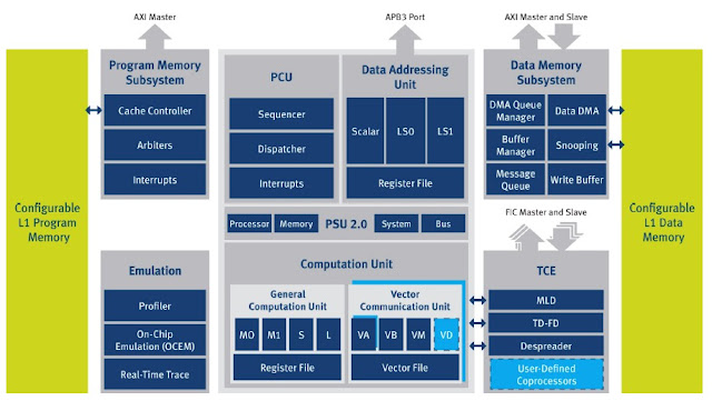
| CEVA is offering the XC4000 in six configurations, with reference architectures for LTE-Advanced and WiFi 802.11ac |
CEVA, a provider of Silicon Intellectual Property (SIP) DSP cores, has announced a new communication engine that will be the successor to the company's XC-323 core , the CEVA-XC4000. CEVA is planning to offer the XC4000 in a series of six programmable DSP cores, targeting applications such as 3G/4G baseband, WiFi connectivity, Bluetooth, Digital TV broadcast demodulation, Smart Grid, White Space and Multimedia over Coax Alliance (MoCA) communications.
Eran Briman, vice president of marketing at CEVA, says that in order to optimize power in the new architecture, the company developed a 2nd-generation Power Scaling Unit (PSU), redesigned the pipeline, and added new features they have named Tightly Couple Extensions (TCE) - which offload the DSP for common modem functions. The result, says Briman, is that the XC4000 achieves 5X the performance of the previous generation XC323 DSP for LTE-Advanced (LTE-A) processing, while consuming 50% less power. CEVA is also introducing two new reference architectures based on the XC4000:
- LTE-A Reference Architecture developed with mimoOn: Release-10 Category-7 FDD worst case (300 / 100 Mbps), with multi-mode support for Time-Domain (TD) LTE-A, HSPA+ Rel-9, TD-SCDMA, and WiMAX. The LTE-A reference architecture supports up to 8x4 MIMO with carrier aggregation of up to two carrier components for a total of 40MHz channel bandwidth.
- WiFi 802.11ac Reference Architecture developed with Antcor: with maximal throughput of 867Mbps (scalable up to 1.7Gbps), supporting up to 4x2 MIMO beam-forming, with 256-QAM support.
CEVA says that fabrication of the LTE-A reference architecture in a 28nm TSMC process will consume a die area of 3.4 sq-mm, a greater than 50% silicon size reduction from the XC323-based PHY in the same process, with just 100mW of power dissipation. The WiFi reference architecture consumes as little as 16mW with 30Mbps Blu-Ray streaming, and occupies a die area of 1.5 sq-mm in a 28nm TSMC process.
The XC4000 employs two computation units, a single general computation unit, and a vector computation unit that can be used in configurations of 1, 2, or 4 cores. The TCEs are coprocessors that execute in parallel with the DSP core. CEVA has developed three TCEs; the Maximum Likelihood Detector (MLD) for Multiple INput-Multiple Output (MIMO) antenna configrations, the Time Domain to Frequency Domain converter (TD-FD), and the Despreader/Descrambler for 3G standards. Users can also add their own TCE coprocessors. CEVA has developed a proprietary low latency Fast Interconnect (FIC) that can support multiple master and slave read/write ports with up to 1.5Tbps data transfer bus with a a bus width of up to 1024 bits.
 |
| The 6 configurations of the CEVA XC4000 cover applications in wireless consumer devices to infrastructure applications |
The six different configurations of the XC4000 which CEVA is introducing vary in terms of number of vector units, Multiply-Accumulate Units (MACs) and data bandwidth. The XC4100, 4110, 4200 and 4210 feature a CEVA fixed point Instruction Set Architecture (ISA), which Briman says is capable of providing floating point (FP) precision. The CEVA-XC4400/4410 includes an IEEE standard floating point unit, targeting infrastructure applications. The 4400/4410 also utilize ARM's Advanced Microcontroller Bus Architecture (AMBA) version 4, for wireless infrastructure requirements.
CEVA is making the XC4000 available to its lead customers in Q1 of 2012, and is targeting general availability for Q2 of 2012.
Related Articles

No comments:
Post a Comment